2002 DODGE RAM differential
[x] Cancel search: differentialPage 211 of 2255
REMOVAL - FRONT ± 2500
(1) Raise and support the vehicle.
(2) Remove the wheel and tire assembly.
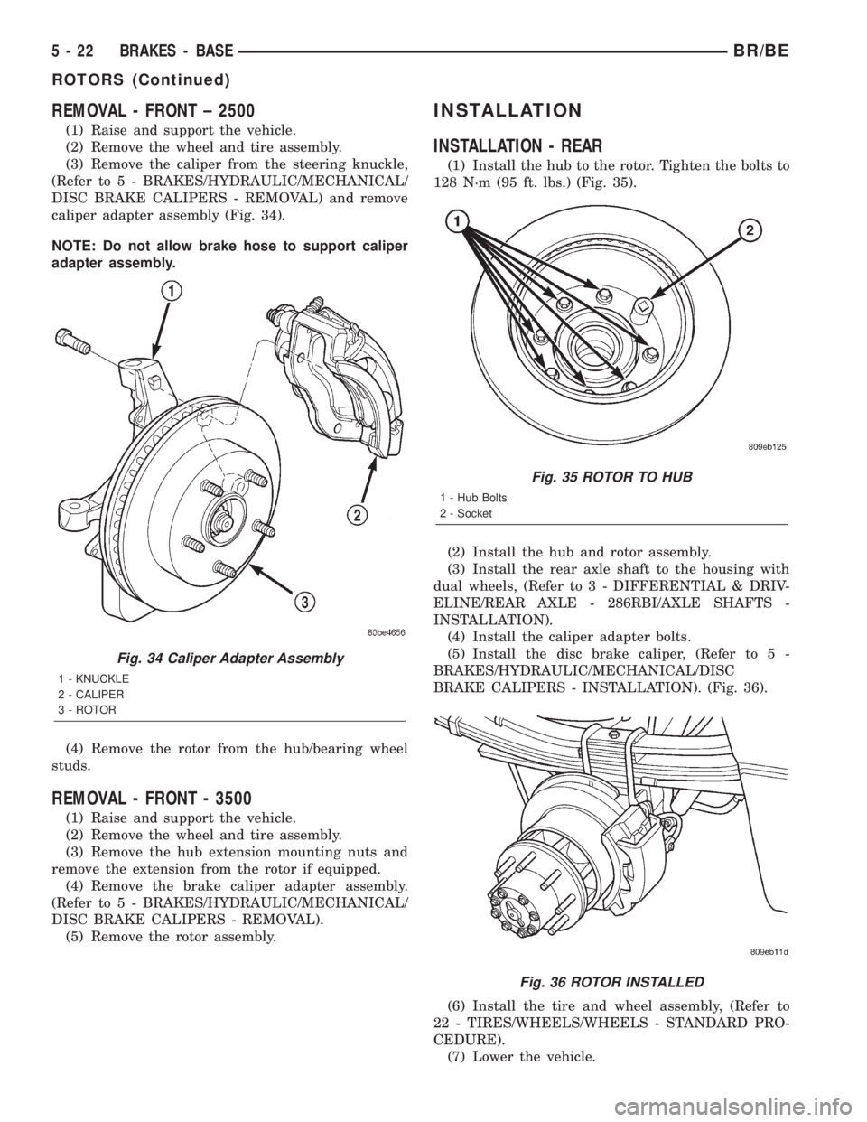
(3) Remove the caliper from the steering knuckle,
(Refer to 5 - BRAKES/HYDRAULIC/MECHANICAL/
DISC BRAKE CALIPERS - REMOVAL) and remove
caliper adapter assembly (Fig. 34).
NOTE: Do not allow brake hose to support caliper
adapter assembly.
(4) Remove the rotor from the hub/bearing wheel
studs.
REMOVAL - FRONT - 3500
(1) Raise and support the vehicle.
(2) Remove the wheel and tire assembly.
(3) Remove the hub extension mounting nuts and
remove the extension from the rotor if equipped.
(4) Remove the brake caliper adapter assembly.
(Refer to 5 - BRAKES/HYDRAULIC/MECHANICAL/
DISC BRAKE CALIPERS - REMOVAL).
(5) Remove the rotor assembly.
INSTALLATION
INSTALLATION - REAR
(1) Install the hub to the rotor. Tighten the bolts to
128 N´m (95 ft. lbs.) (Fig. 35).
(2) Install the hub and rotor assembly.
(3) Install the rear axle shaft to the housing with
dual wheels, (Refer to 3 - DIFFERENTIAL & DRIV-
ELINE/REAR AXLE - 286RBI/AXLE SHAFTS -
INSTALLATION).
(4) Install the caliper adapter bolts.
(5) Install the disc brake caliper, (Refer to 5 -
BRAKES/HYDRAULIC/MECHANICAL/DISC
BRAKE CALIPERS - INSTALLATION). (Fig. 36).
(6) Install the tire and wheel assembly, (Refer to
22 - TIRES/WHEELS/WHEELS - STANDARD PRO-
CEDURE).
(7) Lower the vehicle.
Fig. 34 Caliper Adapter Assembly
1 - KNUCKLE
2 - CALIPER
3 - ROTOR
Fig. 35 ROTOR TO HUB
1 - Hub Bolts
2 - Socket
Fig. 36 ROTOR INSTALLED
5 - 22 BRAKES - BASEBR/BE
ROTORS (Continued)
Page 227 of 2255
FRONT WHEEL SPEED
SENSOR
DESCRIPTION
The ABS brake system uses 3 wheel speed sensors.
A sensor is mounted to each front steering knuckles.
The third sensor is mounted on top of the rear axle
differential housing.
OPERATION
The Wheel Speed Sensor consists of a magnet sur-
rounded by windings from a single strand of wire.
The sensor sends a small AC signal to the CAB. This
signal is generated by magnetic induction. The mag-
netic induction is created when a toothed sensor ring
(exciter ring or tone wheel) passes the stationary
magnetic WSS.
When the ring gear is rotated, the exciter ring
passes the tip of the WSS. As the exciter ring tooth
approaches the tip of the WSS, the magnetic lines of
force expand, causing the magnetic field to cut across
the sensor's windings. This, in turn causes current to
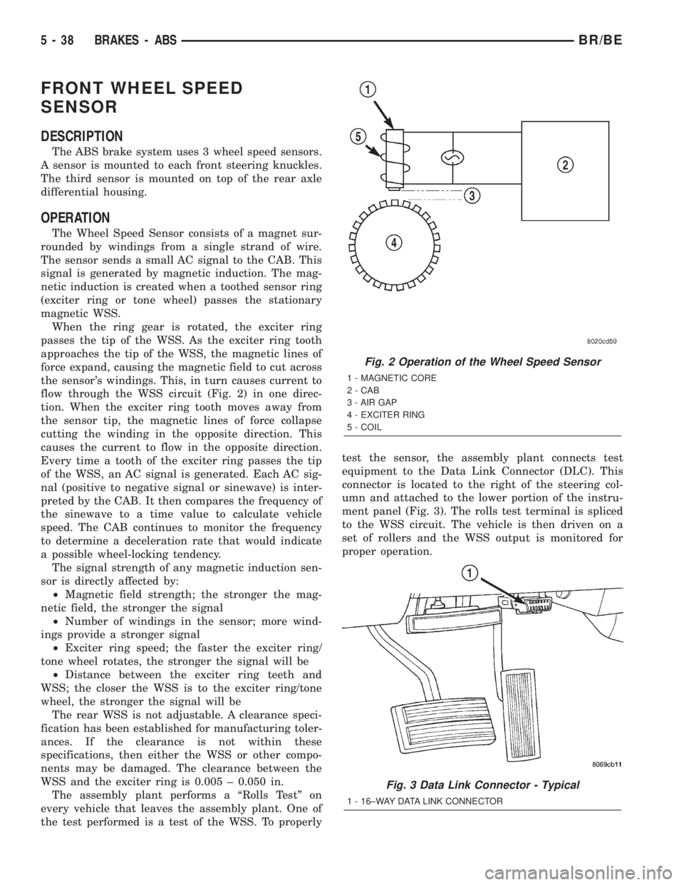
flow through the WSS circuit (Fig. 2) in one direc-
tion. When the exciter ring tooth moves away from
the sensor tip, the magnetic lines of force collapse
cutting the winding in the opposite direction. This
causes the current to flow in the opposite direction.
Every time a tooth of the exciter ring passes the tip
of the WSS, an AC signal is generated. Each AC sig-
nal (positive to negative signal or sinewave) is inter-
preted by the CAB. It then compares the frequency of
the sinewave to a time value to calculate vehicle
speed. The CAB continues to monitor the frequency
to determine a deceleration rate that would indicate
a possible wheel-locking tendency.
The signal strength of any magnetic induction sen-
sor is directly affected by:
²Magnetic field strength; the stronger the mag-
netic field, the stronger the signal
²Number of windings in the sensor; more wind-
ings provide a stronger signal
²Exciter ring speed; the faster the exciter ring/
tone wheel rotates, the stronger the signal will be
²Distance between the exciter ring teeth and
WSS; the closer the WSS is to the exciter ring/tone
wheel, the stronger the signal will be
The rear WSS is not adjustable. A clearance speci-
fication has been established for manufacturing toler-
ances. If the clearance is not within these
specifications, then either the WSS or other compo-
nents may be damaged. The clearance between the
WSS and the exciter ring is 0.005 ± 0.050 in.
The assembly plant performs a ªRolls Testº on
every vehicle that leaves the assembly plant. One of
the test performed is a test of the WSS. To properlytest the sensor, the assembly plant connects test
equipment to the Data Link Connector (DLC). This
connector is located to the right of the steering col-
umn and attached to the lower portion of the instru-
ment panel (Fig. 3). The rolls test terminal is spliced
to the WSS circuit. The vehicle is then driven on a
set of rollers and the WSS output is monitored for
proper operation.
Fig. 2 Operation of the Wheel Speed Sensor
1 - MAGNETIC CORE
2 - CAB
3 - AIR GAP
4 - EXCITER RING
5 - COIL
Fig. 3 Data Link Connector - Typical
1 - 16±WAY DATA LINK CONNECTOR
5 - 38 BRAKES - ABSBR/BE
Page 229 of 2255
NOTE: Check the sensor wire routing. Be sure the
wire is clear of all chassis components and is not
twisted or kinked at any spot.
(6) Install the tire and wheel assembly.
(7) Remove the support and lower the vehicle.
(8) Reconnect the ABS wheel speed sensor wire
electrical connector inside the engine compartment.
(9) Apply the brakes several times to seat the
brake shoes and caliper piston. Do not move the vehi-
cle until a firm brake pedal is obtained.
(10) Verify the wheel speed sensor operation with
a scan tool.
REAR WHEEL SPEED SENSOR
DIAGNOSIS AND TESTING - REAR WHEEL
SPEED SENSOR
Diagnosis of base brake conditions which are
mechanical in nature should be performed first. This
includes brake noise, lack of power assist, parking
brake, or vehicle vibration during normal braking.
The Antilock brake system performs several self-
tests every time the ignition switch is turned on and
the vehicle is driven. The CAB monitors the system
inputs and outputs circuits to verify the system is
operating properly. If the CAB senses a malfunction
in the system it will set a DTC into memory and trig-
ger the warning lamp.
NOTE: The MDS or DRB III scan tool is used to
diagnose the Antilock Brake system. For test proce-
dures refer to the Chassis Diagnostic Manual.
REMOVAL
(1) Raise vehicle on hoist.
(2) Remove brake line mounting nut and remove
the brake line from the sensor stud.
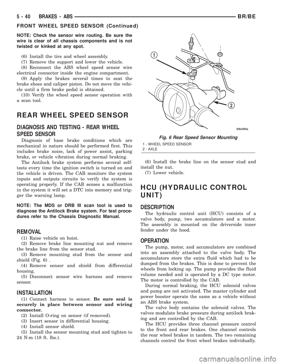
(3) Remove mounting stud from the sensor and
shield (Fig. 6) .
(4) Remove sensor and shield from differential
housing.
(5) Disconnect sensor wire harness and remove
sensor.
INSTALLATION
(1) Connect harness to sensor.Be sure seal is
securely in place between sensor and wiring
connector.
(2) Install O-ring on sensor (if removed).
(3) Insert sensor in differential housing.
(4) Install sensor shield.
(5) Install the sensor mounting stud and tighten to
24 N´m (18 ft. lbs.).(6) Install the brake line on the sensor stud and
install the nut.
(7) Lower vehicle.
HCU (HYDRAULIC CONTROL
UNIT)
DESCRIPTION
The hydraulic control unit (HCU) consists of a
valve body, pump, two accumulators and a motor.
The assembly is mounted on the driverside inner
fender under the hood.
OPERATION
The pump, motor, and accumulators are combined
into an assembly attached to the valve body. The
accumulators store the extra fluid which had to be
dumped from the brakes. This is done to prevent the
wheels from locking up. The pump provides the fluid
volume needed and is operated by a DC type motor.
The motor is controlled by the CAB.
During normal braking, the HCU solenoid valves
and pump are not activated. The master cylinder and
power booster operate the same as a vehicle without
an ABS brake system.
The valve body contains the solenoid valves. The
valves modulate brake pressure during antilock brak-
ing and are controlled by the CAB.
The HCU provides three channel pressure control
to the front and rear brakes. One channel controls
the rear wheel brakes in tandem. The two remaining
channels control the front wheel brakes individually.
Fig. 6 Rear Speed Sensor Mounting
1 - WHEEL SPEED SENSOR
2 - AXLE
5 - 40 BRAKES - ABSBR/BE
FRONT WHEEL SPEED SENSOR (Continued)
Page 372 of 2255

In addition to reducing wire harness complexity,
component sensor current loads and controller hard-
ware, multiplexing offers a diagnostic advantage. A
multiplex system allows the information flowing
between controllers to be monitored using a diagnos-
tic scan tool. The DaimlerChrysler system allows an
electronic control module to broadcast message data
out onto the bus where all other electronic control
modules can ªhearº the messages that are being sent.
When a module hears a message on the data bus
that it requires, it relays that message to its micro-
processor. Each module ignores the messages on the
data bus that are being sent to other electronic con-
trol modules.
With a diagnostic scan tool connected into the CCD
circuit, a technician is able to observe many of the
electronic control module function and message out-
puts while; at the same time, controlling many of the
sensor message inputs. The CCD data bus, along
with the use of a DRBIIItdiagnostic scan tool and a
logic-based approach to test procedures, as found in
the appropriate diagnostic procedures manuals,
allows the trained automotive technician to more eas-
ily, accurately and efficiently diagnose the many com-
plex and integrated electronic functions and features
found on today's vehicles.
OPERATION - CCD DATA BUS
The CCD data bus system was designed to run at a
7812.5 baud rate (or 7812.5 bits per second). In order
to successfully transmit and receive binary messages
over the CCD data bus, the system requires the fol-
lowing:
²Bus (+) and Bus (±) Circuits
²CCD Chips in Each Electronic Control Module
²Bus Bias and Termination
²Bus Messaging
²Bus Message Coding
Following are additional details of each of the
above system requirements.
BUS (+) AND BUS (±) CIRCUITS
The two wires (sometimes referred to as the ªtwist-
ed pairº) that comprise the CCD data bus are the D1
circuit [Bus (+)], and the D2 circuit [Bus (±)]. The9D9
in D1 and D2 identify these as diagnostic circuits.
Transmission and receipt of binary messages on the
CCD data bus is accomplished by cycling the voltage
differential between the Bus (+) and Bus (±) circuits.
The two data bus wires are twisted together in
order to shield the wires from the effects of any Elec-
tro-Magnetic Interference (EMI) from switched volt-
age sources. An induced EMI voltage can be
generated in any wire by a nearby switched voltage
or switched ground circuit. By twisting the data bus
wires together, the induced voltage spike (either upor down) affects both wires equally. Since both wires
are affected equally, a voltage differential still exists
between the Bus (+) and Bus (±) circuits, and the
data bus messages can still be broadcast or received.
The correct specification for data bus wire twisting is
one turn for every 44.45 millimeters (1 ô inches) of
wire.
CCD CHIPS
In order for an electronic control module to commu-
nicate on the CCD data bus, it must have a CCD
chip (Fig. 5). The CCD chip contains a differential
transmitter/receiver (or transceiver), which is used to
send and receive messages. Each module is wired in
parallel to the data bus through its CCD chip.
The differential transceiver sends messages by
using two current drivers: one current source driver,
and one current sink driver. The current drivers are
matched and allow 0.006 ampere to flow through the
data bus circuits. When the transceiver drivers are
turned On, the Bus (+) voltage increases slightly, and
the Bus (±) voltage decreases slightly. By cycling the
drivers On and Off, the CCD chip causes the voltage
on the data bus circuit to fluctuate to reflect the mes-
sage.
Once a message is broadcast over the CCD data
bus, all electronic control modules on the data bus
have the ability to receive it through their CCD chip.
Reception of CCD messages is also carried out by the
transceiver in the CCD chip. The transceiver moni-
tors the voltage on the data bus for any fluctuations.
When data bus voltage fluctuations are detected,
they are interpreted by the transceiver as binary
messages and sent to the electronic control module's
microprocessor.
Fig. 5 CCD Chip
BR/BEELECTRONIC CONTROL MODULES 8E - 7
COMMUNICATION (Continued)
Page 373 of 2255
BUS BIAS AND TERMINATION
The voltage network used by the CCD data bus to
transmit messages requires both bias and termina-
tion. At least one electronic control module on the
data bus must provide a voltage source for the CCD
data bus network known as bus bias, and there must
be at least one bus termination point for the data bus
circuit to be complete. However, while bias and ter-
mination are both required for data bus operation,
they both do not have to be within the same elec-
tronic control module. The CCD data bus is biased to
approximately 2.5 volts. With each of the electronic
control modules wired in parallel to the data bus, all
modules utilize the same bus bias. Therefore, based
upon vehicle options, the data bus can accommodate
two or twenty electronic control modules without
affecting bus voltage.
The power supplied to the data bus is known as
bus biasing. Bus bias is provided through a series cir-
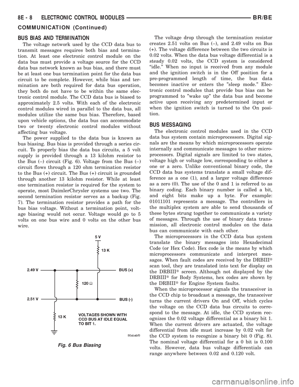
cuit. To properly bias the data bus circuits, a 5 volt
supply is provided through a 13 kilohm resistor to
the Bus (±) circuit (Fig. 6). Voltage from the Bus (±)
circuit flows through a 120 ohm termination resistor
to the Bus (+) circuit. The Bus (+) circuit is grounded
through another 13 kilohm resistor. While at least
one termination resistor is required for the system to
operate, most DaimlerChrysler systems use two. The
second termination resistor serves as a backup (Fig.
7). The termination resistor provides a path for the
bus bias voltage. Without a termination point, volt-
age biasing would not occur. Voltage would go to 5
volts on one bus wire and 0 volts on the other bus
wire.The voltage drop through the termination resistor
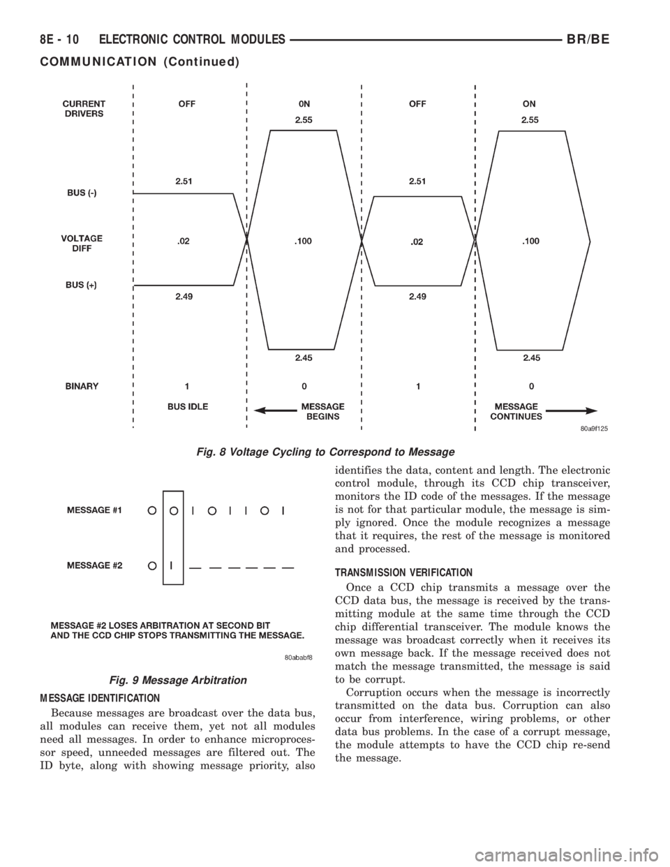
creates 2.51 volts on Bus (±), and 2.49 volts on Bus
(+). The voltage difference between the two circuits is
0.02 volts. When the data bus voltage differential is a
steady 0.02 volts, the CCD system is considered
ªidle.º When no input is received from any module
and the ignition switch is in the Off position for a
pre-programmed length of time, the bus data
becomes inactive or enters the ºsleep mode.º Elec-
tronic control modules that provide bus bias can be
programmed to ºwake upº the data bus and become
active upon receiving any predetermined input or
when the ignition switch is turned to the On posi-
tion.
BUS MESSAGING
The electronic control modules used in the CCD
data bus system contain microprocessors. Digital sig-
nals are the means by which microprocessors operate
internally and communicate messages to other micro-
processors. Digital signals are limited to two states,
voltage high or voltage low, corresponding to either a
one or a zero. Unlike conventional binary code, the
CCD data bus systems translate a small voltage dif-
ference as a one (1), and a larger voltage difference
as a zero (0). The use of the 0 and 1 is referred to as
binary coding. Each binary number is called a bit,
and eight bits make up a byte. For example:
01011101 represents a message. The controllers in
the multiplex system are able to send thousands of
these bytes strung together to communicate a variety
of messages. Through the use of binary data trans-
mission, all electronic control modules on the data
bus can communicate with each other.
The microprocessors in the CCD data bus system
translate the binary messages into Hexadecimal
Code (or Hex Code). Hex code is the means by which
microprocessors communicate and interpret mes-
sages. When fault codes are received by the DRBIIIt
scan tool, they are translated into text for display on
the DRBIIItscreen. Although not displayed by the
DRBIIItfor Body Systems, hex codes are shown by
the DRBIIItfor Engine System faults.
When the microprocessor signals the transceiver in
the CCD chip to broadcast a message, the transceiver
turns the current drivers On and Off, which cycles
the voltage on the CCD data bus circuits to corre-
spond to the message. At idle, the CCD system rec-
ognizes the 0.02 voltage differential as a binary bit 1.
When the current drivers are actuated, the voltage
differential from idle must increase by 0.02 volt for
the CCD system to recognize a binary bit 0 (Fig. 8).
The nominal voltage differential for a 0 bit is 0.100
volts. However, data bus voltage differentials can
range anywhere between 0.02 and 0.120 volt.
Fig. 6 Bus Biasing
8E - 8 ELECTRONIC CONTROL MODULESBR/BE
COMMUNICATION (Continued)
Page 375 of 2255
MESSAGE IDENTIFICATION
Because messages are broadcast over the data bus,
all modules can receive them, yet not all modules
need all messages. In order to enhance microproces-
sor speed, unneeded messages are filtered out. The
ID byte, along with showing message priority, alsoidentifies the data, content and length. The electronic
control module, through its CCD chip transceiver,
monitors the ID code of the messages. If the message
is not for that particular module, the message is sim-
ply ignored. Once the module recognizes a message
that it requires, the rest of the message is monitored
and processed.
TRANSMISSION VERIFICATION
Once a CCD chip transmits a message over the
CCD data bus, the message is received by the trans-
mitting module at the same time through the CCD
chip differential transceiver. The module knows the
message was broadcast correctly when it receives its
own message back. If the message received does not
match the message transmitted, the message is said
to be corrupt.
Corruption occurs when the message is incorrectly
transmitted on the data bus. Corruption can also
occur from interference, wiring problems, or other
data bus problems. In the case of a corrupt message,
the module attempts to have the CCD chip re-send
the message.
Fig. 8 Voltage Cycling to Correspond to Message
Fig. 9 Message Arbitration
8E - 10 ELECTRONIC CONTROL MODULESBR/BE
COMMUNICATION (Continued)
Page 376 of 2255

DIAGNOSIS AND TESTING - CCD DATA BUS
CCD BUS FAILURE
The CCD data bus can be monitored using the
DRBIIItscan tool. However, it is possible for the
data bus to pass all tests since the voltage parame-
ters will be in ªrangeª and false signals are being
sent. There are essentially 12 ªhard failuresª that
can occur with the CCD data bus:
²Bus Shorted to Battery
²Bus Shorted to 5 Volts
²Bus Shorted to Ground
²Bus (+) Shorted to Bus (±)
²Bus (±) and Bus (+) Open
²Bus (+) Open
²Bus (±) Open
²No Bus Bias
²Bus Bias Level Too High
²Bus Bias Level Too Low
²No Bus Termination
²Not Receiving Bus Messages Correctly
Refer to the appropriate diagnostic information for
details on how to diagnose these faults using a
DRBIIItscan tool.
BUS FAILURE VISUAL SYMPTOM DIAGNOSIS
The following visible symptoms or customer com-
plaints, alone or in combination, may indicate a CCD
data bus failure:
²Airbag Indicator and Malfunction Indicator
Lamp (MIL) Illuminated
²Instrument Cluster Gauges (All) Inoperative
²No Compass Mini-Trip Computer (CMTC) Oper-
ation (if equipped)
CONTROLLER ANTILOCK
BRAKE
DESCRIPTION
The Controller Antilock Brakes (CAB) is a micro-
processor which handles testing, monitoring and con-
trolling the ABS brake system operation (Fig. 10).
The CAB functions are:
²Perform self-test diagnostics.
²Monitor the RWAL brake system for proper oper-
ation.
²Control the RWAL valve solenoids.
NOTE: If the CAB needs to be replaced, the rear
axle type and tire revolutions per mile must be pro-
gramed into the new CAB. For axle type refer to
Group 3 Differential and Driveline. For tire revolu-
tions per mile,(Refer to 22 - TIRES/WHEELS/TIRES -
SPECIFICATIONS) . To program the CAB refer to the
Chassis Diagnostic Manual.
OPERATION
SYSTEM SELF-TEST
When the ignition switch is turned-on the micro-
processor RAM and ROM are tested. If an error
occurs during the test, a DTC will be set into the
RAM memory. However it is possible the DTC will
not be stored in memory if the error has occurred in
the RAM module were the DTC's are stored. Also it
is possible a DTC may not be stored if the error has
occurred in the ROM which signals the RAM to store
the DTC.
CAB INPUTS
The CAB continuously monitors the speed of the
differential ring gear by monitoring signals generated
by the rear wheel speed sensor. The CAB determines
a wheel locking tendency when it recognizes the ring
gear is decelerating too rapidly. The CAB monitors
the following inputs to determine when a wheel lock-
ing tendency may exists:
²Rear Wheel Speed Sensor
²Brake Lamp Switch
²Brake Warning Lamp Switch
²Reset Switch
²4WD Switch (If equipped)
CAB OUTPUTS
The CAB controls the following outputs for antilock
braking and brake warning information:
²RWAL Valve
²ABS Warning Lamp
²Brake Warning Lamp
REMOVAL
(1) Disconnect battery negative cable.
Fig. 10 RWAL CAB
1-RWALCAB
BR/BEELECTRONIC CONTROL MODULES 8E - 11
COMMUNICATION (Continued)
Page 508 of 2255
disconnect mechanism, (Refer to 3 - DIFFERENTIAL
& DRIVELINE/FRONT AXLE/AXLE VACUUM
MOTOR - OPERATION). The four-wheel drive switch
input to the instrument cluster circuitry can be diag-
nosed using conventional diagnostic tools and meth-
ods.
DIAGNOSIS AND TESTING - FOUR-WHEEL
DRIVE INDICATOR
The diagnosis found here addresses an inoperative
four-wheel drive indicator condition. If the problem
being diagnosed is related to indicator accuracy, be
certain to confirm that the problem is with the indi-
cator and not with a damaged or inoperative front
axle disconnect mechanism. (Refer to 3 - DIFFEREN-
TIAL & DRIVELINE/FRONT AXLE/AXLE VACUUM
MOTOR - DIAGNOSIS AND TESTING). If no front
axle disconnect problem is found, the following proce-
dure will help locate a short or open in the four-
wheel drive switch input to the instrument cluster.
Refer to the appropriate wiring information. The wir-
ing information includes wiring diagrams, proper
wire and connector repair procedures, details of wire
harness routing and retention, connector pin-out
information and location views for the various wire
harness connectors, splices and grounds.
WARNING: ON VEHICLES EQUIPPED WITH AIR-
BAGS, DISABLE THE AIRBAG SYSTEM BEFORE
ATTEMPTING ANY STEERING WHEEL, STEERING
COLUMN, OR INSTRUMENT PANEL COMPONENT
DIAGNOSIS OR SERVICE. DISCONNECT AND ISO-
LATE THE BATTERY NEGATIVE (GROUND) CABLE,
THEN WAIT TWO MINUTES FOR THE AIRBAG SYS-
TEM CAPACITOR TO DISCHARGE BEFORE PER-
FORMING FURTHER DIAGNOSIS OR SERVICE. THIS
IS THE ONLY SURE WAY TO DISABLE THE AIRBAG
SYSTEM. FAILURE TO TAKE THE PROPER PRE-
CAUTIONS COULD RESULT IN ACCIDENTAL AIR-
BAG DEPLOYMENT AND POSSIBLE PERSONAL
INJURY.
INDICATOR DOES NOT ILLUMINATE WITH FOUR-WHEEL
DRIVE MODE SELECTED
(1) Disconnect and isolate the battery negative
cable. Disconnect the engine wire harness connector
for the four-wheel drive switch from the switch con-
nector receptacle. Check for continuity between the
ground circuit cavity of the engine wire harness con-
nector for the four-wheel drive switch and a good
ground. There should be continuity. If OK, go to Step
2. If not OK, repair the open ground circuit to ground
(G100) as required.
(2) Reconnect the battery negative cable. Turn the
ignition switch to the On position. Install a jumper
wire between the 4WD switch sense circuit cavity ofthe engine wire harness connector for the four-wheel
drive switch and a good ground. The four-wheel drive
indicator should light. If OK, replace the faulty four-
wheel drive switch. If not OK, go to Step 3.
(3) Turn the ignition switch to the Off position.
Disconnect and isolate the battery negative cable.
Remove the instrument cluster from the instrument
panel. Check for continuity between the 4WD switch
sense circuit cavities of the instrument panel wire
harness connector (Connector C2) for the instrument
cluster and the engine wire harness connector for the
four-wheel drive switch. There should be continuity.
If OK, replace the faulty instrument cluster. If not
OK, repair the open 4WD switch sense circuit
between the instrument cluster and the four-wheel
drive switch as required.
INDICATOR STAYS ILLUMINATED WITH FOUR-WHEEL DRIVE
MODE NOT SELECTED
(1) Disconnect and isolate the battery negative
cable. Disconnect the engine wire harness connector
for the four-wheel drive switch from the switch con-
nector receptacle. Check for continuity between the
ground circuit terminal and the 4WD switch sense
circuit terminal in the four-wheel drive switch con-
nector receptacle. There should be no continuity. If
OK, repair the shorted 4WD switch sense circuit
between the four-wheel drive switch and the instru-
ment cluster as required. If not OK, replace the
faulty four-wheel drive switch.
SPEEDOMETER
DESCRIPTION
A speedometer is standard equipment on all instru-
ment clusters. The speedometer is located just to the
right of the tachometer near the center of the instru-
ment cluster. The speedometer consists of a movable
gauge needle or pointer controlled by the instrument
cluster circuitry and a fixed 210 degree primary scale
on the gauge dial face that reads left-to-right either
from 0 to 120 mph, or from 0 to 200 km/h, depending
upon the market for which the vehicle is manufac-
tured. Each version also has a secondary inner scale
on the gauge dial face that provides the equivalent
opposite units from the primary scale. Text appearing
on the cluster overlay just below the hub of the
speedometer needle abbreviates the unit of measure
for the primary scale in all upper case letters (i.e.:
MPH or KM/H), followed by the unit of measure for
the secondary scale in all lower case letters (i.e.: mph
or km/h). The speedometer graphics are white (pri-
mary scale) and red (secondary scale) against a black
field, making them clearly visible within the instru-
ment cluster in daylight. When illuminated from
behind by the panel lamps dimmer controlled cluster
BR/BEINSTRUMENT CLUSTER 8J - 29
SHIFT INDICATOR (TRANSFER CASE) (Continued)