2001 DODGE RAM differential
[x] Cancel search: differentialPage 292 of 2889
REMOVAL - REAR - 2500/3500
(1) Raise and support the vehicle
(2) Remove the tire and wheel assembly.
(3) Remove the disc brake caliper, (Refer to 5 -
BRAKES/HYDRAULIC/MECHANICAL/DISC
BRAKE CALIPERS - REMOVAL).
(4) Remove the caliper adapter bolts.
(5) Remove the rear axle shaft from the housing
on dual rear wheels, (Refer to 3 - DIFFERENTIAL &
DRIVELINE/REAR AXLE - 286RBI/AXLE SHAFTS -
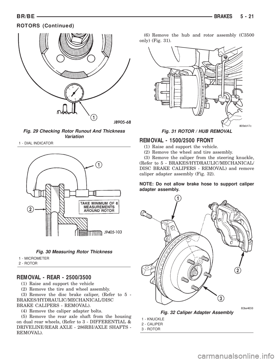
REMOVAL).(6) Remove the hub and rotor assembly (C3500
only) (Fig. 31).
REMOVAL - 1500/2500 FRONT
(1) Raise and support the vehicle.
(2) Remove the wheel and tire assembly.
(3) Remove the caliper from the steering knuckle,
(Refer to 5 - BRAKES/HYDRAULIC/MECHANICAL/
DISC BRAKE CALIPERS - REMOVAL) and remove
caliper adapter assembly (Fig. 32).
NOTE: Do not allow brake hose to support caliper
adapter assembly.
Fig. 29 Checking Rotor Runout And Thickness
Variation
1 - DIAL INDICATOR
Fig. 30 Measuring Rotor Thickness
1 - MICROMETER
2 - ROTOR
Fig. 31 ROTOR / HUB REMOVAL
Fig. 32 Caliper Adapter Assembly
1 - KNUCKLE
2 - CALIPER
3 - ROTOR
BR/BEBRAKES 5 - 21
ROTORS (Continued)
Page 293 of 2889
(4) Remove the rotor from the hub/bearing wheel
studs.
REMOVAL - 3500 FRONT
(1) Raise and support the vehicle.
(2) Remove the wheel and tire assembly.
(3) Remove the hub extension mounting nuts and
remove the extension from the rotor if equipped.
(4) Remove the brake caliper adapter assembly.
(Refer to 5 - BRAKES/HYDRAULIC/MECHANICAL/
DISC BRAKE CALIPERS - REMOVAL).
(5) Remove the rotor assembly.
INSTALLATION - REAR - 2500/3500
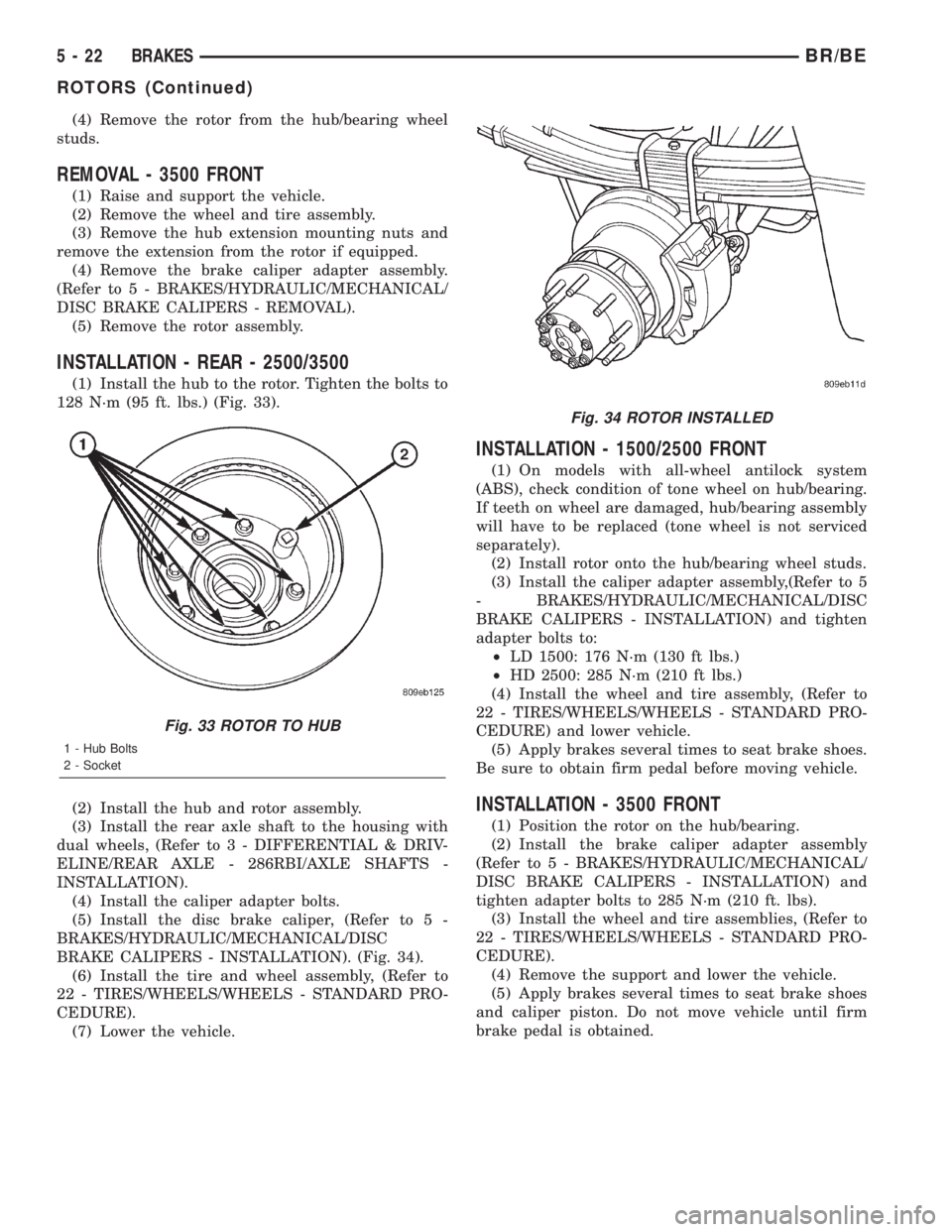
(1) Install the hub to the rotor. Tighten the bolts to
128 N´m (95 ft. lbs.) (Fig. 33).
(2) Install the hub and rotor assembly.
(3) Install the rear axle shaft to the housing with
dual wheels, (Refer to 3 - DIFFERENTIAL & DRIV-
ELINE/REAR AXLE - 286RBI/AXLE SHAFTS -
INSTALLATION).
(4) Install the caliper adapter bolts.
(5) Install the disc brake caliper, (Refer to 5 -
BRAKES/HYDRAULIC/MECHANICAL/DISC
BRAKE CALIPERS - INSTALLATION). (Fig. 34).
(6) Install the tire and wheel assembly, (Refer to
22 - TIRES/WHEELS/WHEELS - STANDARD PRO-
CEDURE).
(7) Lower the vehicle.
INSTALLATION - 1500/2500 FRONT
(1) On models with all-wheel antilock system
(ABS), check condition of tone wheel on hub/bearing.
If teeth on wheel are damaged, hub/bearing assembly
will have to be replaced (tone wheel is not serviced
separately).
(2) Install rotor onto the hub/bearing wheel studs.
(3) Install the caliper adapter assembly,(Refer to 5
- BRAKES/HYDRAULIC/MECHANICAL/DISC
BRAKE CALIPERS - INSTALLATION) and tighten
adapter bolts to:
²LD 1500: 176 N´m (130 ft lbs.)
²HD 2500: 285 N´m (210 ft lbs.)
(4) Install the wheel and tire assembly, (Refer to
22 - TIRES/WHEELS/WHEELS - STANDARD PRO-
CEDURE) and lower vehicle.
(5) Apply brakes several times to seat brake shoes.
Be sure to obtain firm pedal before moving vehicle.
INSTALLATION - 3500 FRONT
(1) Position the rotor on the hub/bearing.
(2) Install the brake caliper adapter assembly
(Refer to 5 - BRAKES/HYDRAULIC/MECHANICAL/
DISC BRAKE CALIPERS - INSTALLATION) and
tighten adapter bolts to 285 N´m (210 ft. lbs).
(3) Install the wheel and tire assemblies, (Refer to
22 - TIRES/WHEELS/WHEELS - STANDARD PRO-
CEDURE).
(4) Remove the support and lower the vehicle.
(5) Apply brakes several times to seat brake shoes
and caliper piston. Do not move vehicle until firm
brake pedal is obtained.
Fig. 33 ROTOR TO HUB
1 - Hub Bolts
2 - Socket
Fig. 34 ROTOR INSTALLED
5 - 22 BRAKESBR/BE
ROTORS (Continued)
Page 458 of 2889

In addition to reducing wire harness complexity,
component sensor current loads and controller hard-
ware, multiplexing offers a diagnostic advantage. A
multiplex system allows the information flowing
between controllers to be monitored using a diagnos-
tic scan tool. The Chrysler system allows an elec-
tronic control module to broadcast message data out
onto the bus where all other electronic control mod-
ules can ªhearº the messages that are being sent.
When a module hears a message on the data bus
that it requires, it relays that message to its micro-
processor. Each module ignores the messages on the
data bus that are being sent to other electronic con-
trol modules.
With a diagnostic scan tool connected into the CCD
circuit, a technician is able to observe many of the
electronic control module function and message out-
puts while; at the same time, controlling many of the
sensor message inputs. The CCD data bus, along
with the use of a diagnostic scan tool and a logic-
based approach to test procedures, as found in the
Diagnostic Procedures manuals, allows the trained
automotive technician to more easily, accurately and
efficiently diagnose the many complex and integrated
electronic functions and features found on today's
vehicles.
OPERATION - CCD DATA BUS
The CCD data bus system was designed to run at a
7812.5 baud rate (or 7812.5 bits per second). In order
to successfully transmit and receive binary messages
over the CCD data bus, the system requires the fol-
lowing:
²Bus (+) and Bus (±) Circuits
²CCD Chips in Each Electronic Control Module
²Bus Bias and Termination
²Bus Messaging
²Bus Message Coding
Following are additional details of each of the
above system requirements.
BUS (+) AND BUS (±) CIRCUITS
The two wires (sometimes referred to as the ªtwist-
ed pairº) that comprise the CCD data bus are the D1
circuit [Bus (+)], and the D2 circuit [Bus (±)]. The9D9
in D1 and D2 identify these as diagnostic circuits.
Transmission and receipt of binary messages on the
CCD data bus is accomplished by cycling the voltage
differential between the Bus (+) and Bus (±) circuits.The two data bus wires are twisted together in
order to shield the wires from the effects of any Elec-
tro-Magnetic Interference (EMI) from switched volt-
age sources. An induced EMI voltage can be
generated in any wire by a nearby switched voltage
or switched ground circuit. By twisting the data bus
wires together, the induced voltage spike (either up
or down) affects both wires equally. Since both wires
are affected equally, a voltage differential still exists
between the Bus (+) and Bus (±) circuits, and the
data bus messages can still be broadcast or received.
The correct specification for data bus wire twisting is
one turn for every 44.45 millimeters (1
3¤4inches) of
wire.
CCD CHIPS
In order for an electronic control module to commu-
nicate on the CCD data bus, it must have a CCD
chip (Fig. 5). The CCD chip contains a differential
transmitter/receiver (or transceiver), which is used to
send and receive messages. Each module is wired in
parallel to the data bus through its CCD chip.
The differential transceiver sends messages by
using two current drivers: one current source driver,
and one current sink driver. The current drivers are
matched and allow 0.006 ampere to flow through the
data bus circuits. When the transceiver drivers are
turned On, the Bus (+) voltage increases slightly, and
the Bus (±) voltage decreases slightly. By cycling the
drivers On and Off, the CCD chip causes the voltage
on the data bus circuit to fluctuate to reflect the mes-
sage.
Fig. 5 CCD Chip
BR/BEELECTRONIC CONTROL MODULES 8E - 7
COMMUNICATION (Continued)
Page 459 of 2889
Once a message is broadcast over the CCD data
bus, all electronic control modules on the data bus
have the ability to receive it through their CCD chip.
Reception of CCD messages is also carried out by the
transceiver in the CCD chip. The transceiver moni-
tors the voltage on the data bus for any fluctuations.
When data bus voltage fluctuations are detected,
they are interpreted by the transceiver as binary
messages and sent to the electronic control module's
microprocessor.
BUS BIAS AND TERMINATION
The voltage network used by the CCD data bus to
transmit messages requires both bias and termina-
tion. At least one electronic control module on the
data bus must provide a voltage source for the CCD
data bus network known as bus bias, and there must
be at least one bus termination point for the data bus
circuit to be complete. However, while bias and ter-
mination are both required for data bus operation,
they both do not have to be within the same elec-
tronic control module. The CCD data bus is biased to
approximately 2.5 volts. With each of the electronic
control modules wired in parallel to the data bus, all
modules utilize the same bus bias. Therefore, based
upon vehicle options, the data bus can accommodate
two or twenty electronic control modules without
affecting bus voltage.
The power supplied to the data bus is known as
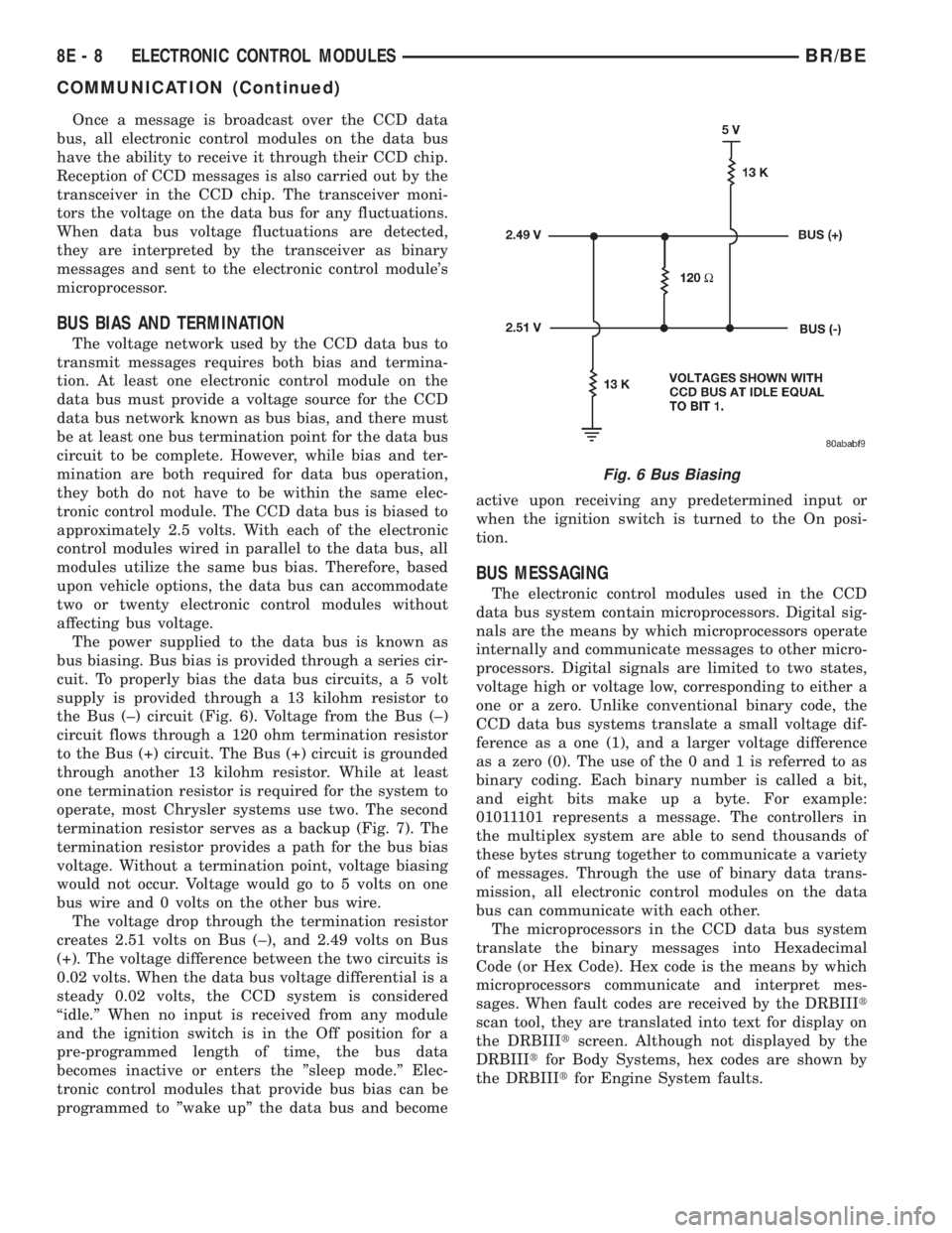
bus biasing. Bus bias is provided through a series cir-
cuit. To properly bias the data bus circuits, a 5 volt
supply is provided through a 13 kilohm resistor to
the Bus (±) circuit (Fig. 6). Voltage from the Bus (±)
circuit flows through a 120 ohm termination resistor
to the Bus (+) circuit. The Bus (+) circuit is grounded
through another 13 kilohm resistor. While at least
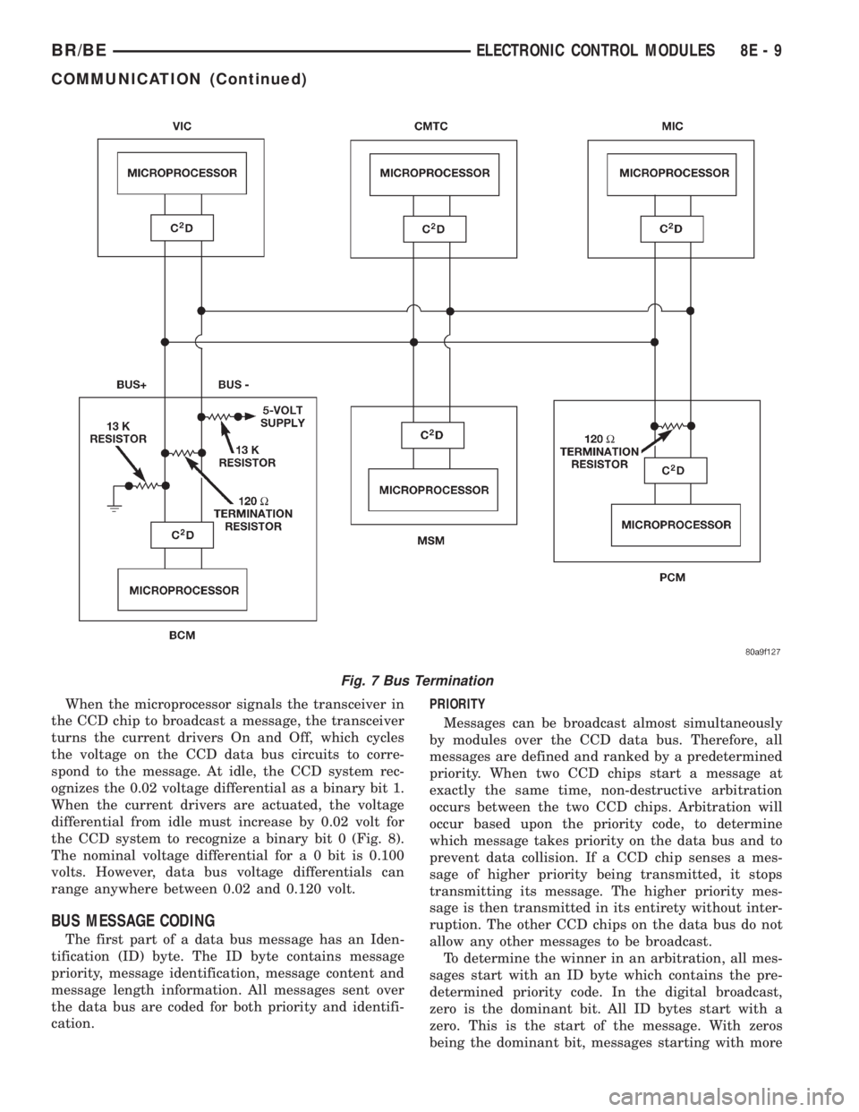
one termination resistor is required for the system to
operate, most Chrysler systems use two. The second
termination resistor serves as a backup (Fig. 7). The
termination resistor provides a path for the bus bias
voltage. Without a termination point, voltage biasing
would not occur. Voltage would go to 5 volts on one
bus wire and 0 volts on the other bus wire.
The voltage drop through the termination resistor
creates 2.51 volts on Bus (±), and 2.49 volts on Bus
(+). The voltage difference between the two circuits is
0.02 volts. When the data bus voltage differential is a
steady 0.02 volts, the CCD system is considered
ªidle.º When no input is received from any module
and the ignition switch is in the Off position for a
pre-programmed length of time, the bus data
becomes inactive or enters the ºsleep mode.º Elec-
tronic control modules that provide bus bias can be
programmed to ºwake upº the data bus and becomeactive upon receiving any predetermined input or
when the ignition switch is turned to the On posi-
tion.
BUS MESSAGING
The electronic control modules used in the CCD
data bus system contain microprocessors. Digital sig-
nals are the means by which microprocessors operate
internally and communicate messages to other micro-
processors. Digital signals are limited to two states,
voltage high or voltage low, corresponding to either a
one or a zero. Unlike conventional binary code, the
CCD data bus systems translate a small voltage dif-
ference as a one (1), and a larger voltage difference
as a zero (0). The use of the 0 and 1 is referred to as
binary coding. Each binary number is called a bit,
and eight bits make up a byte. For example:
01011101 represents a message. The controllers in
the multiplex system are able to send thousands of
these bytes strung together to communicate a variety
of messages. Through the use of binary data trans-
mission, all electronic control modules on the data
bus can communicate with each other.
The microprocessors in the CCD data bus system
translate the binary messages into Hexadecimal
Code (or Hex Code). Hex code is the means by which
microprocessors communicate and interpret mes-
sages. When fault codes are received by the DRBIIIt
scan tool, they are translated into text for display on
the DRBIIItscreen. Although not displayed by the
DRBIIItfor Body Systems, hex codes are shown by
the DRBIIItfor Engine System faults.
Fig. 6 Bus Biasing
8E - 8 ELECTRONIC CONTROL MODULESBR/BE
COMMUNICATION (Continued)
Page 460 of 2889
When the microprocessor signals the transceiver in
the CCD chip to broadcast a message, the transceiver
turns the current drivers On and Off, which cycles
the voltage on the CCD data bus circuits to corre-
spond to the message. At idle, the CCD system rec-
ognizes the 0.02 voltage differential as a binary bit 1.
When the current drivers are actuated, the voltage
differential from idle must increase by 0.02 volt for
the CCD system to recognize a binary bit 0 (Fig. 8).
The nominal voltage differential for a 0 bit is 0.100
volts. However, data bus voltage differentials can
range anywhere between 0.02 and 0.120 volt.
BUS MESSAGE CODING
The first part of a data bus message has an Iden-
tification (ID) byte. The ID byte contains message
priority, message identification, message content and
message length information. All messages sent over
the data bus are coded for both priority and identifi-
cation.PRIORITY
Messages can be broadcast almost simultaneously
by modules over the CCD data bus. Therefore, all
messages are defined and ranked by a predetermined
priority. When two CCD chips start a message at
exactly the same time, non-destructive arbitration
occurs between the two CCD chips. Arbitration will
occur based upon the priority code, to determine
which message takes priority on the data bus and to
prevent data collision. If a CCD chip senses a mes-
sage of higher priority being transmitted, it stops
transmitting its message. The higher priority mes-
sage is then transmitted in its entirety without inter-
ruption. The other CCD chips on the data bus do not
allow any other messages to be broadcast.
To determine the winner in an arbitration, all mes-
sages start with an ID byte which contains the pre-
determined priority code. In the digital broadcast,
zero is the dominant bit. All ID bytes start with a
zero. This is the start of the message. With zeros
being the dominant bit, messages starting with more
Fig. 7 Bus Termination
BR/BEELECTRONIC CONTROL MODULES 8E - 9
COMMUNICATION (Continued)
Page 461 of 2889
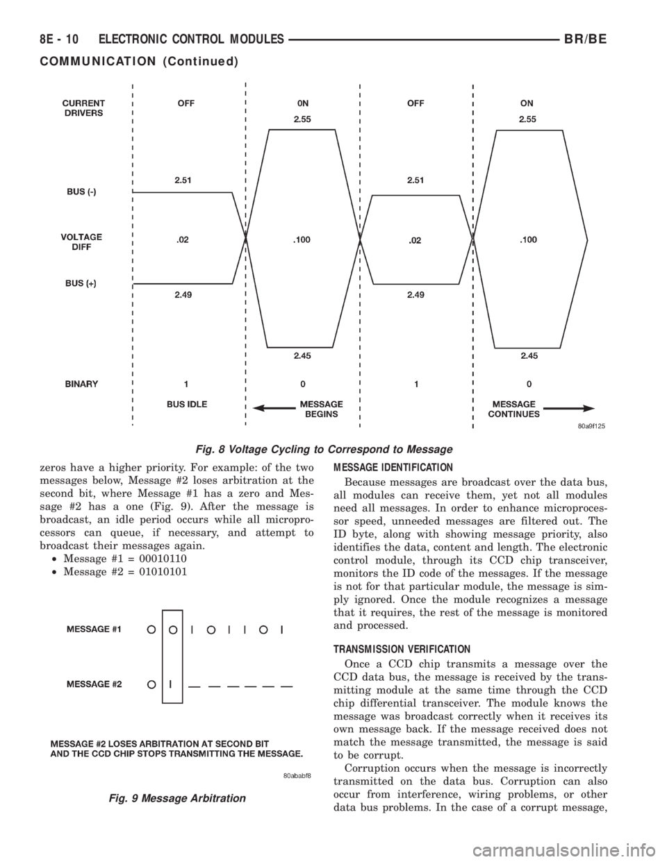
zeros have a higher priority. For example: of the two
messages below, Message #2 loses arbitration at the
second bit, where Message #1 has a zero and Mes-
sage #2 has a one (Fig. 9). After the message is
broadcast, an idle period occurs while all micropro-
cessors can queue, if necessary, and attempt to
broadcast their messages again.
²Message #1 = 00010110
²Message #2 = 01010101MESSAGE IDENTIFICATION
Because messages are broadcast over the data bus,
all modules can receive them, yet not all modules
need all messages. In order to enhance microproces-
sor speed, unneeded messages are filtered out. The
ID byte, along with showing message priority, also
identifies the data, content and length. The electronic
control module, through its CCD chip transceiver,
monitors the ID code of the messages. If the message
is not for that particular module, the message is sim-
ply ignored. Once the module recognizes a message
that it requires, the rest of the message is monitored
and processed.
TRANSMISSION VERIFICATION
Once a CCD chip transmits a message over the
CCD data bus, the message is received by the trans-
mitting module at the same time through the CCD
chip differential transceiver. The module knows the
message was broadcast correctly when it receives its
own message back. If the message received does not
match the message transmitted, the message is said
to be corrupt.
Corruption occurs when the message is incorrectly
transmitted on the data bus. Corruption can also
occur from interference, wiring problems, or other
data bus problems. In the case of a corrupt message,
Fig. 8 Voltage Cycling to Correspond to Message
Fig. 9 Message Arbitration
8E - 10 ELECTRONIC CONTROL MODULESBR/BE
COMMUNICATION (Continued)
Page 462 of 2889

the module attempts to have the CCD chip re-send
the message.
DIAGNOSIS AND TESTING - CCD DATA BUS
CCD BUS FAILURE
The CCD data bus can be monitored using the
DRBIIItscan tool. However, it is possible for the
data bus to pass all tests since the voltage parame-
ters will be in ªrangeª and false signals are being
sent. There are essentially 12 ªhard failuresª that
can occur with the CCD data bus:
²Bus Shorted to Battery
²Bus Shorted to 5 Volts
²Bus Shorted to Ground
²Bus (+) Shorted to Bus (±)
²Bus (±) and Bus (+) Open
²Bus (+) Open
²Bus (±) Open
²No Bus Bias
²Bus Bias Level Too High
²Bus Bias Level Too Low
²No Bus Termination
²Not Receiving Bus Messages Correctly
Refer to the appropriate diagnostic procedures for
details on how to diagnose these faults using a
DRBIIItscan tool.
BUS FAILURE VISUAL SYMPTOM DIAGNOSIS
The following visible symptoms or customer com-
plaints, alone or in combination, may indicate a CCD
data bus failure:
²Airbag Indicator Lamp and Malfuntion Indicator
Lamp (MIL) Illuminated
²Instrument Cluster Gauges (All) Inoperative
²No Compass Mini-Trip Computer (CMTC) Oper-
ation
CONTROLLER ANTILOCK
BRAKE
DESCRIPTION
The Controller Antilock Brakes (CAB) is a micro-
processor which handles testing, monitoring and con-
trolling the ABS brake system operation (Fig. 10).
The CAB functions are:
²Perform self-test diagnostics.
²Monitor the RWAL brake system for proper oper-
ation.
²Control the RWAL valve solenoids.
NOTE: If the CAB needs to be replaced, the rear
axle type and tire revolutions per mile must be pro-
gramed into the new CAB. For axle type refer to
Group 3 Differential and Driveline. For tire revolu-tions per mile,(Refer to 22 - TIRES/WHEELS/TIRES -
SPECIFICATIONS) . To program the CAB refer to the
Chassis Diagnostic Manual.
OPERATION
SYSTEM SELF-TEST
When the ignition switch is turned-on the micro-
processor RAM and ROM are tested. If an error
occurs during the test, a DTC will be set into the
RAM memory. However it is possible the DTC will
not be stored in memory if the error has occurred in
the RAM module were the DTC's are stored. Also it
is possible a DTC may not be stored if the error has
occurred in the ROM which signals the RAM to store
the DTC.
CAB INPUTS
The CAB continuously monitors the speed of the
differential ring gear by monitoring signals generated
by the rear wheel speed sensor. The CAB determines
a wheel locking tendency when it recognizes the ring
gear is decelerating too rapidly. The CAB monitors
the following inputs to determine when a wheel lock-
ing tendency may exists:
²Rear Wheel Speed Sensor
²Brake Lamp Switch
²Brake Warning Lamp Switch
²Reset Switch
²4WD Switch (If equipped)
CAB OUTPUTS
The CAB controls the following outputs for antilock
braking and brake warning information:
²RWAL Valve
Fig. 10 RWAL CAB
1-RWALCAB
BR/BEELECTRONIC CONTROL MODULES 8E - 11
COMMUNICATION (Continued)
Page 588 of 2889
SHIFT INDICATOR (TRANSFER
CASE)
DESCRIPTION
A four-wheel drive indicator is standard equipment
on all instrument clusters. However, on vehicles not
equipped with the optional four-wheel drive system,
this indicator is mechanically disabled. The four-
wheel drive indicator is located near the lower edge
of the instrument cluster overlay, to the right of cen-
ter. The four-wheel drive indicator consists of a sten-
cilled cutout of the text ª4WDº in the opaque layer of
the instrument cluster overlay. The dark outer layer
of the overlay prevents the indicator from being
clearly visible when it is not illuminated. An amber
lens behind the cutout in the opaque layer of the
overlay causes the ª4WDº text to appear in amber
through the translucent outer layer of the overlay
when the indicator is illuminated from behind by a
Light Emitting Diode (LED) soldered onto the instru-
ment cluster electronic circuit board. The four-wheel
drive indicator is serviced as a unit with the instru-
ment cluster.
OPERATION
The four-wheel drive indicator lamp gives an indi-
cation to the vehicle operator that a four-wheel drive
operating mode is engaged. The indicator will be illu-
minated when either high range (4H) or low range
(4L) have been selected with the transfer case shift
lever. This indicator is controlled by a transistor on
the instrument cluster circuit board based upon the
cluster programming, and a hard wired input from
the four-wheel drive switch on the front axle discon-
nect housing. The four-wheel drive indicator Light
Emitting Diode (LED) receives battery current on the
instrument cluster electronic circuit board through
the fused ignition switch output (st-run) circuit
whenever the ignition switch is in the On or Start
positions; therefore, the lamp will always be off when
the ignition switch is in any position except On or
Start. The LED only illuminates when it is switched
to ground by the instrument cluster transistor.
The four-wheel drive switch is connected in series
between ground and the four-wheel drive switch
sense input to the instrument cluster. For further
information on the transfer case and the transfer
case operating ranges, (Refer to 21 - TRANSMIS-
SION/TRANSAXLE/TRANSFER CASE - OPERA-
TION. For further information on the front axle
disconnect mechanism, (Refer to 3 - DIFFERENTIAL
& DRIVELINE/FRONT AXLE/AXLE VACUUM
MOTOR - OPERATION). The four-wheel drive switch
input to the instrument cluster circuitry can be diag-nosed using conventional diagnostic tools and meth-
ods.
DIAGNOSIS AND TESTING - FOUR-WHEEL
DRIVE INDICATOR
The diagnosis found here addresses an inoperative
four-wheel drive indicator condition. If the problem
being diagnosed is related to indicator accuracy, be
certain to confirm that the problem is with the indi-
cator and not with a damaged or inoperative front
axle disconnect mechanism. (Refer to 3 - DIFFEREN-
TIAL & DRIVELINE/FRONT AXLE/AXLE VACUUM
MOTOR - DIAGNOSIS AND TESTING). If no front
axle disconnect problem is found, the following proce-
dure will help locate a short or open in the four-
wheel drive switch input to the instrument cluster.
Refer to the appropriate wiring information. The wir-
ing information includes wiring diagrams, proper
wire and connector repair procedures, details of wire
harness routing and retention, connector pin-out
information and location views for the various wire
harness connectors, splices and grounds.
WARNING: ON VEHICLES EQUIPPED WITH AIR-
BAGS, DISABLE THE AIRBAG SYSTEM BEFORE
ATTEMPTING ANY STEERING WHEEL, STEERING
COLUMN, OR INSTRUMENT PANEL COMPONENT
DIAGNOSIS OR SERVICE. DISCONNECT AND ISO-
LATE THE BATTERY NEGATIVE (GROUND) CABLE,
THEN WAIT TWO MINUTES FOR THE AIRBAG SYS-
TEM CAPACITOR TO DISCHARGE BEFORE PER-
FORMING FURTHER DIAGNOSIS OR SERVICE. THIS
IS THE ONLY SURE WAY TO DISABLE THE AIRBAG
SYSTEM. FAILURE TO TAKE THE PROPER PRE-
CAUTIONS COULD RESULT IN ACCIDENTAL AIR-
BAG DEPLOYMENT AND POSSIBLE PERSONAL
INJURY.
INDICATOR DOES NOT ILLUMINATE WITH FOUR-WHEEL
DRIVE MODE SELECTED
(1) Disconnect and isolate the battery negative
cable. Disconnect the engine wire harness connector
for the four-wheel drive switch from the switch con-
nector receptacle. Check for continuity between the
ground circuit cavity of the engine wire harness con-
nector for the four-wheel drive switch and a good
ground. There should be continuity. If OK, go to Step
2. If not OK, repair the open ground circuit to ground
(G100) as required.
(2) Reconnect the battery negative cable. Turn the
ignition switch to the On position. Install a jumper
wire between the 4WD switch sense circuit cavity of
the engine wire harness connector for the four-wheel
drive switch and a good ground. The four-wheel drive
indicator should light. If OK, replace the faulty four-
wheel drive switch. If not OK, go to Step 3.
BR/BEINSTRUMENT CLUSTER 8J - 29